OUR TECHNOLOGY
State-of-the-art nanoscale and atomic level imaging and characterization are significant challenges for science and engineering. Advances in new materials, devices, and cell biology that span all engineering and science disciplines are predicated on understanding fundamental structure-composition-property relationships. The Transmission Electron Microscope (TEM) has become ubiquitous for directly imaging and understanding the properties of materials at the atomic scale. Wavik's cornerstone product, the Vesta® laser sample heating system, was originally developed for the TEM, and is now also available for the SEM, FIB and HIM.
The Vesta® system relies on Waviks expertise in fully programmable nanomanipulators and the physics of nanoanalysis. The Vesta® system produces a very small (10 um) heated area on the sample, so fast temperature ramping is easy and multiple sites on the same sample can be examined. There is no thermal damage to detectors or the column, and there is minimal thermal-mechanical drift in the sample, so long duration studies and movies are easy. The laser can be pulsed to look at transient events. On the analytical side, EEGS (Electron Energy Gain Spectroscopy) with laser stimulation is possible.
IN THE NEWS

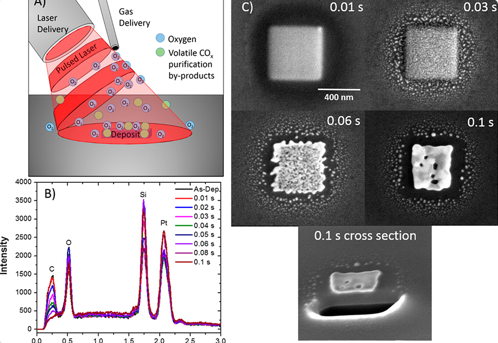
ELECTRON BEAM INDUCED DEPOSITION PURIFICATION VIA PULSED LASER INDUCED OXIDATION REACTION
Teams from Oak Ridge National Laboratory, University of Tennessee, Utah State University, and Graz University of Technology demonstrated electron beam induced deposition purification via pulsed laser induced oxidation reaction using the Waviks Vesta.

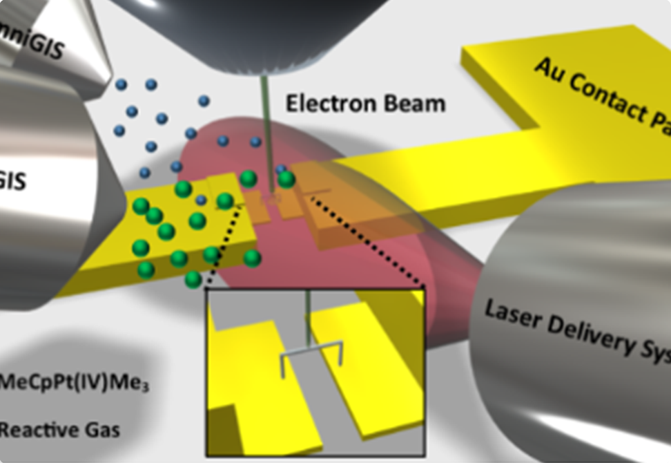
EXPLORING PHOTOTHERMAL PATHWAYS VIA IN SITU LASER HEATING THE TEM
Collaborators from University of Notre Dame, University of Tennessee, and Oak Ridge National Lab explored photothermal heating pathways using the Waviks Vesta. Their work was published in Microscopy and Microanalysis.

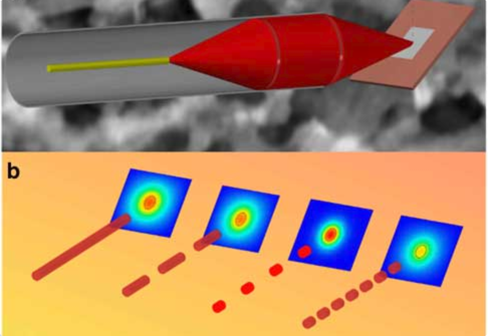
3D NANOPRINTING VIA LASER-ASSISTED ELECTRON BEAM INDUCED DEPOSITION
Teams from University of Tennessee, Graz Centre for Electron Microscopy, and Oak Ridge National Lab explored 3D nanoprinting via laser-assisted electron beam induced deposition. Their work was published in the Beilstein Journal of Nanotechnology.
Contact us to learn more
Required fields are marked *
